
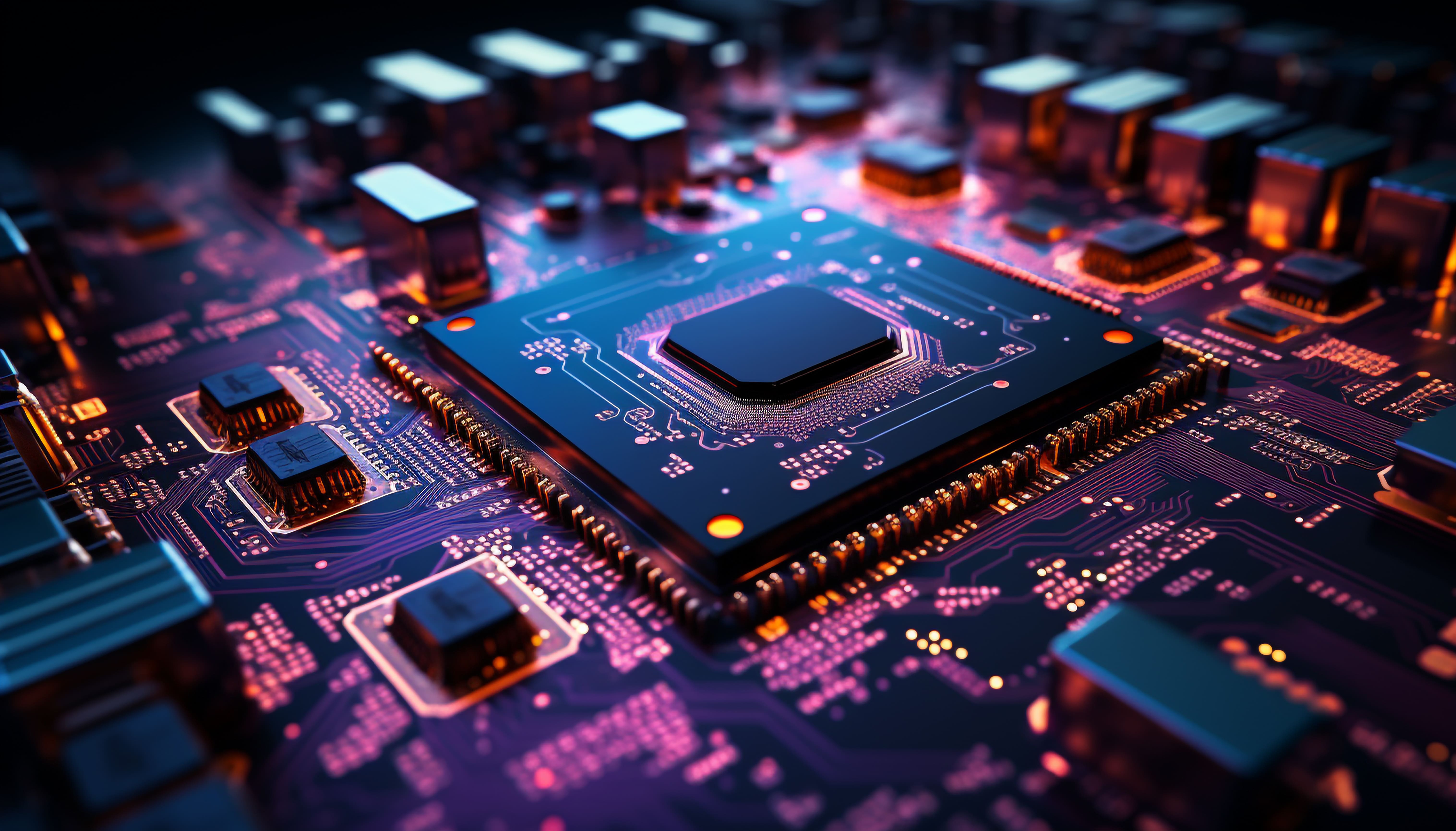
Top 10 Emerging Trends In VLSI In 2024
VLSI is a process of creating an Integrated Circuit By Combining Millions Of Transistors Into A Single Chip. Most ICS had limited functionality before the invention of the VLSI. VLSI has changed the way we think of technology today. VLSI allows IC designers to merge RAM, ROM, and other logic into single chip.
In this blog topic we will be discussing upon the Emerging VLSI trends in 2024
1. 3D ICs and Heterogeneous Integration: A three-dimensional integrated circuit is a Metal Oxide Semiconductor (MOS) integrated circuit whereby one can stack as many as 16 ICs and interconnect them vertically, for instance, using silicon via or copper; unlike the traditional 2D integrated circuits, that are laid flat in a single plane, 3D ICs stack multiple active electronic component layers vertically. This stacking can significantly enhance performance, reduce power consumption, and decrease the overall footprint of the IC.
These different advantages of using the 3D ICs and Heterogeneous Circuits include Lower Power Consumption, Faster Signal Transitions, Analog and Digital Integration, and Space Savings. In 2d ICS multiple Different functional layers, for instance, logic, memory, and sensors, can all be interconnected by this new philosophy, reducing interconnect lengths while increasing communication density as is the case in 3d IC Circuits.
2. EUV Lithography: Extreme Ultraviolet is a new technology in semiconductor manufacturing that aids in creating very small features on silicon wafers. This technology is one step toward the creation of modern microchips, which can bring life to everything from smartphones to high-performance computing systems. In the past few decades—or, at most, since the 1960s—it has been possible to fit more than 50 billion transistors into a single chip using 2 nanometre technology. EUV resorts to extreme ultraviolet lithography in the production of integrated circuits.
How EUV Lithography works?
EUV lithography systems emit light with wavelengths of about 13.5 nanometers, which is considerably shorter than the wavelength used in the previous generation of DUV lithography. EUV Lithography enables shorter wavelengths and helps gap between two transistors much finer
3. AI and Machine Learning in VLSI Design: AI And ML In VLSI Design Invloves- Enhanced Automation, Better Design Quality: Less Time-to-Market, Cost Savings and .
Scalability. AI techniques can also be used to optimize some aspects of VLSI design, such as with genetic algorithms. Many VLSI techniques can be incorporated, which make the chip layout and design compact and efficient. RTL ML Algorithms can ensure design specifications and performance goals. It can also aid in the physical design improvement and enhancement, thus helping to take up issues of optimizing the chip layout for such integrated circuits. Other design challenges that AI can help tackle are those involving signal integrity analysis and clock tree synthesis.
4. Quantum Processors: Quantum processors are the basic elements of a quantum computer that execute computations based on the principles set by quantum mechanics. They are extremely different from classical processors and have an overall potential for efficiently solving certain types of problems. What is important in quantum processors or quantum computing is the number of quibits because it exponentially enhances the power of computation of the quantum computing chip.
It is these spin qubits, relatively tiny in size, which only measures 100 nm across, making them denser than other qubit types. The fabrication approach was conducted in a process using extreme ultraviolet lithography. If there is anything that is going to ascertain a future for quantum computing, it will have to be the ability to fabricate quantum computing chips with an ever-increasing number of qubits.
5. Advanced Transistor Architectures: Moore's Law predicts that the number of transistors on a microchip doubles about every two years. For the continuance of Moore's Law, advanced transistor architectures are required. Some new architectures have been developed, aimed at improving performance and reducing power consumption for scaling, as planar traditional transistors are reaching both physical and performance limits.
A steeper transistor count could be achieved by stacking and merging the transistors in a vertical fashion. The proposed architecture is known as complementary field effect transistor
CFET requires a new set of metal wiring along with the power rails used to power up the device.
6. Neuromorphic Computing: This is the newest frontier of computing, fostered by the structure and functionality of the human brain to make it more efficient, more adaptable, and strong in computational power for specific tasks. Neuromorphic computing or neuromorphic processors use chip architecture that combines both memory and processor. Researchers have also reported increasingly creative ways to mimic the brain's architecture using artificial components, including memristors, capacitors, spintronic devices, and even some interesting attempts to implement neuromorphic computing
The term neuromorphic computing refers to the process of designing of both hardware and software computing elements
7. Brain-Inspired Chips: A brain-inspired chip is over 20 times as fast as—and roughly 25 times as energy-efficient as—any microchip currently available on the market, when performing artificial intelligence tasks. The Key concepts of neuromorphic computing and brain inspired chips are
Neurons and Synapses:
Neurons: These are the basic processing units in the brain. In neuromorphic chips, they are represented by artificial neurons, which do the computations.
Synapses: The connections between neurons along which the signal travels. Artificial synapses, just like synaptic plasticity in the brain, adjust the strength of the connection with the signal in a neuromorphic chip.
Optical Interconnects: Any system that transmits signals from one part of an integrated circuit to another by light is an optical interconnect. Optical interconnects are mostly based on optical fibers.
In computing systems of VLSI, computer-generated holograms are used to configure optical interconnects. This paper has shown that replacing some of the electronic interconnects with interconnects that introduce free-space optical communications paths can better interconnect devices on one chip or wafer and chips or modules.
9. Circuits That Stretch: It comprises a large variety of technologies for constructing electronic circuits by deposition or embedding of electronic devices and circuits onto elastic or stretchable substrates. Also, it is known as elastic electronics or elastic circuits.
Some benefits of stretchable include lightweight, high-performance, and low manufacturing costs, thus fueling market growth. These are used in wearable communication devices, bio-integrated circuits, and robotic sensory skin.
10. Hardware Security: This is the security of the physical devices, systems, and hardware components from unauthorized access, tampering, and other malicious activities.
Key Areas of Hardware Security in VLSI
1.Physical Unclonable Functions (PUFs)
2.Hardware Trojans
3.Side-Channel Attacks:
4.Reverse Engineering:
5.Secure Design and Verification:
6.Trusted Execution Environments (TEEs):
Reviews